Import
Import BruceThe Import Module converts output data from an Electronic CAD system to a Macaos Enterprise product. In most cases, you will be importing a set of Gerber and Drill files. Each of these files must be linked to the correct layer of the PCB. It is also necessary to specify the desired stackup for the product, and perhaps some other properties as well.
The Import Module also supports importing ODB++ data. In an ODB++ dataset, the graphic data is already linked to specific layers. This layer linking should be checked (and corrected, if necessary) before specifying product properties.
You can also add fiducial marks and other symbols to the product prior to publishing. There are also tools for inspecting and measuring features of the product.
Once a product has been completely specified, you must save the product so that it will be available for panelization, creating a solder paste stencil or in-circuit test fixture, working with assembly data, etc.
Creating a board product
Creating a board product BruceIn most cases, you can use the following procedure to create a board product:
- Open the data files. When you open the Import Module, select the zip file (or the individual files) for the product. The Import Module will attempt to autolink each file to the appropriate layer based on the names of the individual files. The files are listed in the Files pane.
- Check the file – layer linking. Files which are not autolinked must be linked manually, by clicking on the blue text in the Layer column of the Files pane and selecting the desired layer from the layer menu. The file image is displayed, in order to help select the correct layer. Right-click on a file to view the file as text or to change the file type.
- Review drill holes. In most cases drill files are read and interpreted correctly. But you should check that this is the case. You can modify tool diameters in the Drills pane. If necessary, see Scale adjustment and Offset adjustment for information on how to make adjustments. Be sure to also check/correct plating for each tool, and drill depth for each file. Right-click on a tool to specify via plugging/filling for all holes with that tool.
- Define the board contour. Go to the Board outline pane. In many cases, the outer contour and inner contour (if any) will be defined automatically. If so, this should be checked to insure that the contour was defined correctly. Track routing and scoring (if any) must always be defined manually.
- Place the product/batch number. The manufacturer usually adds a product/batch number to the board. You may specify its position by clicking on the No. icon button and placing the rectangle at the desired position on the board.
- Specify the board parameters.
- Go to the Specs pane. You must select a stackup. In addition, you may choose non-standard surface finish, solder mask color and legend color and various other specifications. If the product is to have electrolytic (hard) gold applied to any pads or connector surfaces, then the gold area (in cm²) must also be specified.
- Go to the Stats pane. Minimum track width, clearance and annular ring must be specified for the product. Correct the estimated values if necessary.
- Go to the ID & Options pane. You must specify a product name. You may also specify an article number and description and select options.
- Publish the product. Choose File|Publish to Product Browser to publish the new product:
- Go through each item in the approval checklist to insure that you haven't forgotten anything. Click the OK button to continue.
- Once the product has been published to the server, the new product number will be displayed. You'll find the product in the Never Ordered folder and Recently Published folder of the product browser.
Linking files
Linking files BruceThe Files pane lists the files which have been added to the project using the File|Add files command. Each file is listed together with its file type and the layer to which the file has been linked. Multiple files may be selected when opening files. Additional files may be added executing the File|Add files command again.
When a file is added to the list, an attempt is made to determine the file type. If, for some reason, the file type is incorrect, it can be changed by right-clicking on the file and choosing the correct file type from the Change file type submenu. (Note: Empty image files are identified as text files.)
The contents of the file list may be filtered with the Configure menu:
- Configure|Hide linked files hides all files that have already been linked
- Configure|Hide non-image files hides all text files and other non-image files
- Configure|Hide common part of file names shows only the portion of filenames used by autolinking
Image files
Image files BruceClicking on an image file imports the file into the system (if necessary) and displays the file in the Graphic Display. Macaos Enterprise is able to import the following image file formats:
- Basic Gerber (RS-274D)
- Gerber (RS-274X Extended Gerber)
- NC Drill (XNC, Excellon or similar; drill only)
- Sieb & Meyer (drill only)
- Excellon (with limited support for rout instructions)
- ODB++ files (in a zip, gzip, tar or tgz archive). See ODB++ for more info.
-
IPC-D-356 (bare-board test data). See the IPC-D-356 section for more info.
To import Basic Gerber files you must specify several extra parameters. There may also be difficulties interpreting incomplete Drill files, as explained in Drill Tools.
To link a file to a layer, click on the layer name (or Not Selected) and choose the desired layer from the menu. To unlink a file, choose Not used.
Normally, only Drill files should be linked to a drill layer. Some CAD systems generate Gerber files of drill drawings or drill templates, which are intended for paper documentation purposes. Attempting to link a Gerber file which contains lines, arcs or polygons to a drill layer (Additional layers|Drill) will probably give undesirable results. If your CAD system outputs a drill file in Gerber, then the Gerber file must only contain pads (flashes) where the pad diameters are equal to the hole diameters. Note: Use Additional layers|Drill drawing to link Gerber drill drawings for documentation purposes.
An image file showing which drill holes should be filled or plugged should be linked to the appropriate via protection layer (tented, plugged, filled or capped) in the Additional layers submenu. See Via protection for more info.
If while preparing a product for import, you discover that a layer needs to be updated, you can replace that layer without having to restart the entire import process. Right-click on the file name and choose Replace file. Note: It is not possible to replace the board/contour file. If this file needs to be updated then the entire product must be imported again.
Sometimes, it may be necessary to use the same file for two different layers. For example, you may have only one solder mask file, which is to be used both for the top and bottom layers. To solve this problem, right-click on the file name and choose Duplicate file. This will add a copy of the file to the list, which can then be linked to another layer.
When an image file is imported into the system, warnings and errors (if any) are stored in a report which can be viewed by right-clicking on the file name and choosing View file import report.
Note: All of the Gerber files must have the same coordinate origin. If necessary, you will need to change the setup of your CAD system so that the files have the same origin.
Note: Some CAD systems mirror alternate Gerber layers when they are generated. The import module is not able to correct for this, since it is not possible to automatically determine the mirroring axis. All Gerber files must have the same coordinate origin and mirror state.
Note: Normally, only image files are included when a product is saved or published. Non-image files may be viewed locally while preparing the product. To force a non-image file to be included, assign it to a Documentation or Assembly layer. See Non-image files.
Basic Gerber files
Basic Gerber files BruceBasic Gerber files contain only x-y coordinates and device codes. In order for these files to be interpreted, there are a number of parameters which must be defined externally to the coordinate file. When importing a Basic Gerber file, the Specify coordinate format dialog box must be filled out so that the file can be interpretated correctly. There are four parameters which must be specified. Usually, these settings can be determined from the Gerber Export settings of the CAD program which generated the files.
If you are unable to determine the correct parameters, then you should try the default values and check carefully that the resulting image has the correct size and shape. The Specify coordinate format dialog box explains the meaning and consequences of each parameter in greater detail.
Once the coordinate format has been specified, it will be used for any additional Gerber files that are imported; until the File|New Product command is executed or the Import Module is closed.
Basic Gerber files also need an Aperture Table, which lists the sizes and shapes of the “Apertures” (or drawing shapes) referred to by the device codes in the coordinate file. Sometimes, Basic Gerber files are generated in accordance with a standardized table, such as NOR01 or PERFAG-10a, but most CAD systems generate a separate aperture file (or wheel file or tool report) together with the Basic Gerber files.
If undefined apertures are encountered while importing a Basic Gerber file, the Specify aperture table dialog box opens. This dialog box lists the undefined device codes (apertures) which were found in the coordinate file. The upper left region lists standardized aperture tables as well as all non-image files listed in the Files pane. Clicking one one of these files causes the file contents to be displayed in the upper right region.
Nearly every CAD system generates aperture files differently. Once you have located the correct aperture file, you should choose the parser for your CAD system from the list in the lower left region. The parsed aperture table will then be shown in the lower right region. Once an aperture table is located that defines all of the undefined apertures listed at the top of the dialog box, the OK button is enabled.
Note: It is sometimes possible to come up with a valid aperture table even though the wrong aperture file or the wrong parser is used. If you are unsure of the aperture table, you should inspect the graphic display carefully to insure that the Basic Gerber files have been interpreted properly.
If the coordinate format or aperture table was not correctly specified, choose File|New Product and repeat the import process with the correct parameters.
HP-GL plotter files
HP-GL plotter files BruceThe Import Module has limited support for plotter files in HP-GL format. HP-GL files may be included in a product for documentation purposes only.
Due to the nature of the HP-GL format it is not possible to reliably detect an HP-GL file without parsing the entire file. Therefore, the Import Module detects HP-GL files as Text (or Other, if the file contains plotter setup escape sequences).
To view an HP-GL file, right-click on the file name and choose Change file type|HP-GL. The file will be displayed in the viewer.
To include the file in a product, link the file to a User layer. It is not possible to link an HP-GL file to any other layer.
The HP-GL parser supports only a subset of HP-GL commands. In particular, there is no support for fonts, line styles, wedges or filling of polygons. Unsupported commands are ignored, which may give undesirable results.
DXF Files
DXF Files BruceThe Import Module has limited support for 2D CAD drawings in DXF format. DXF files may be included in a product for documentation purposes only.
To include a DXF file in a product, link the file to a User layer. It is not possible to link a DXF file to any other layer.
The DXF parser supports only a subset of DXF entities and parameters. Unsupported entities include all 3D, view, text and dimenson entities. In addition, entities which use elliptical or spline curves are not supported. The parser interprets all dimensions as mm, unless the $INSUNITS parameter is set to 1 (inch). Unsupported entities are ignored, which may give undesirable results.
Non-image files
Non-image files BruceOften, it is desirable to include documentation files together with the image files. For example, assembly instructions, drawings, pick and place data, etc should be included in the product so that an EMS provider can purchase PCBs and process component assembly with one set of data.
By default, non-image files are ignored when publishing a product. However, if non-image files are assigned to a Documentation or Assembly layer, then they will be included in the product. You should avoid linking unnecessary files as Documentation files.
Assembly files are given standardized filenames in the product. For this reason, only one file should be assigned to an assembly layer since duplicate filenames will cause some files to be ignored. Note: PnP and BOM data are added to the board as component layers, rather than as separate files.
In the Macaos Enterprise product viewer, documentation files are listed below the layer list. Double-click on a filename to open the file, or right-click on the filename to save the file.
ODB++ files
ODB++ files BruceWhen opening an ODB++ project, the layers, outer contour and drill tools are automatically imported and linked. The layers in from the ODB++ project are listed in the ODB++ Layers pane.
If a layer has been linked incorrectly, right-click to link it to a different layer.
If the board has inner contours, track routing or scoring, then these must be specified in the normal manner. The stackup, finish and mask colors must also be specified.
If the ODB++ project contains multiple steps, you must choose which step to open. In most cases, one step will be the board and another step will be a panel containing the board. If you are unsure which step to open, choose any step. After viewing the step, you can reopen the file to view a different step, if necessary. The import module has some limitations when working with panelized steps, so we recommend importing the board step and using the Panelization module to create your panel.
If the file archive containing the ODB++ project also contains other files, these will be listed below the list of ODB++ layers. You may double-click on a file in this list to view the file. All files in this list are saved with the product when publishing.
Note: Import of ODB++ files is a relatively new technology in the Import module. We recommend that you inspect your board carefully before publishing. If you encounter problems, you can help us improve the ODB++ engine by using the Help|Send problem report command to send us your files together with a description of the problem.
Note: The Macaos ODB++ engine is not able to read files in the discontinued and unsupported XML-based ODB++(X) format.
IPC-D-356 files
IPC-D-356 files BruceWhen opening an IPC-D-356 file, the bare-board test pads for both the top and bottom sides are extracted to the Test pads top and Test pads bottom layers, respectively. The net name, designator and pin number is also extracted for each test pad. Other information in the IPC-D-356 file is ignored.
Note: Do not confuse test pads with test points or test pins.
-
Test pads are the locations for bare-board testing of the PCB during manufacture, which are extracted from an IPC-D-356 file to the Test pads layers.
-
Test points are specific pads or pins on the PCBA which would be used for in-circuit testing. For each test point, a “component” (with the Test point component class) should be added to the appropriate component layer. Ideally, test points (with TPxx designators) should be included in Pick and Place data, but they may also be created manually.
-
Test pins are the pins in a test fixture which will make contact with the PCBA during in-circuit testing.
In the Assembly Data Manager (ADM), information from the test pads is used to specify the outline and the location of the key pin for components where this information is lacking.
In the Test fixtures Designer, information from the test pads is used to specify the designator, pin number and net name for test pins where this information is lacking.
An IPC-D-356 file contains important information for electrical test of the bare PCB during manufacture. Since only a subset of this information is imported to the test pads layers, the complete file is also attached to the product, so that it is available to the manufacturer.
Pick and place data
Pick and place data BruceWhen a pick and place (PnP) data file is assigned to a Component layer, the Import Module will attempt to interpret the data. If the file format is not immediately recognized, then it may be specified in the Pick and Place Data Import dialog box, which displays the original file contents, parsed file contents and the interpreted XYR data.
The following may be specified:
-
Number of header lines
-
First character of comment lines
-
Separated or fixed-width columns
-
Separator and quote characters (for separated files)
-
Column widths (for fixed-width files)
-
Unit of measure for X and Y coordinates
-
Angle rotation direction (counter-clockwise or clockwise)
-
Column mapping. (Up to 3 columns may be combined as the component description.)
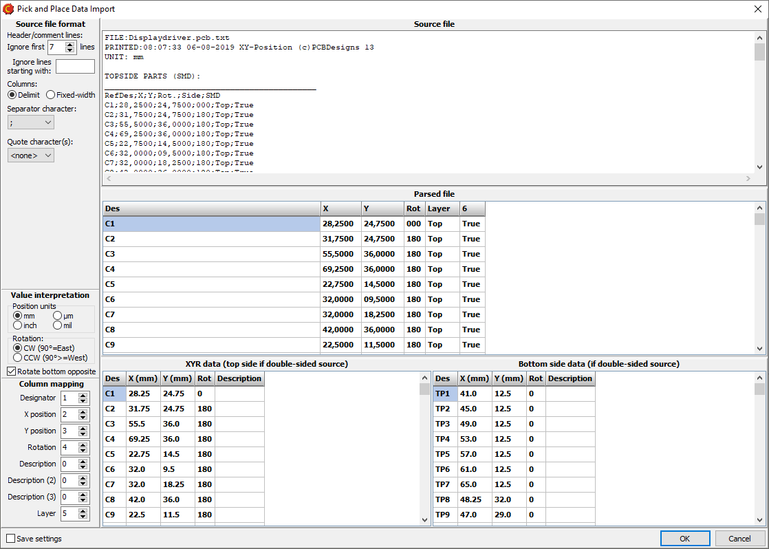
Once the data has been parsed, the components are added to the Component Top and/or Component Bottom layers.
Note: A component layer may not have duplicate component designators. When importing specifications for a component which already exists, the component properties are updated with the imported data.
If the PnP data does not have the same coordinate origin as the Gerber data, then the component symbols will be offset from their correct position on the board. This may be corrected by aligning the component data with the Gerber data.
Bill of Materials
Bill of Materials BruceA bill of materials (BOM) may be imported to a component layer from a spreadsheet or a text file. For best results, the outer contour of the PCB should be defined, and pick and place data should be imported, before importing a BOM.
When importing a text file, the file format must be specified. Choose between delimited or fixed-width fields. For delimeted fields, the delimiter character must be specified. For fixed-width fields, click on the ruler to specify the column widths. Note: Ignore the First row headers and Ignore first rows settings. These are managed in the next step.
The Import BOM dialog box is used to convert imported data to the Macaos component structure. The source data is shown in the upper grid and the parsed data is shown in the lower grid.
If the first row contains column headers, then an attempt is made to automatically link columns in the upper grid to columns in the lower grid. If necessary, specify rows in the upper grid to ignore.
The lower grid columns must be linked to their corresponding columns in the upper grid. If the column does not exist in the upper grid, then it should be mapped to column zero.
If a row contains multiple designators, then the separator character must be specified. Otherwise, this field should be left empty.
If a source column has both supplier name and supplier part number (SKU) in the same column, then the separator character should be specified. Otherwise, this field should be left empty.
If necessary, it is possible to add data to individual cells in the lower grid. Simply click on the cell and start typing to replace all text in the cell. Alternatively, click 3 times to place the cursor at the desired position in the text of the cell.
Each row in the Parsed BOM must have a unique designator. A warning is generated if empty or duplicate designator cells are found when attempting to save the imported BOM data.
Click the OK button to import the parsed BOM data.
The designator is the unique identifier for each component. For components which already exist on one of the component layers, the component’s properties are updated with the values from the imported BOM. New components are added to the left of the PCB with 10 mm spacing.
After the PCB has been published, the Assembly Data Manager module may be used to inspect and modify component data, as well as to export PnP and BOM data in various formats.
Layers
Layers BruceA printed circuit board is made up of several “layers”. These include copper layers, mask and legend layers, drill files and more. Each layer is described by one (or sometimes two) image files, and normally a file describes only one layer. The Layer overview shows the filenames and layer names of the board. The check boxes for each layer may be used to view or hide the layer in the graphic display. The rectangle to the right of the check box shows the color used to display the layer in the Graphic Display. You can right-click on this rectangle to change the color.
The Route layer is automatically generated by adding contour objects (in the Contour pane).
The controls at the top of the Layer Overview may be used to specify the number of copper layers on the board. This is automatically increased if you link additional layers in the Files pane. However, if you want to reduce the number of copper layers, you must do so here.
For single layer boards, it is not possible to link a soldermask file to the non-copper side of the board. In the Board Specifications pane, the soldermask color for the non-copper side will be set to None. Changing this to another color will indicate that the board should have soldermask on the non-copper side.
You may right-click on the layer overview to quickly show only top layers, only bottom layers, all layers or no layers.
Autolink
Autolink BruceAutolinking is a process of mapping files to the correct layers of the board. The import module is designed to support Gerber and Drill files from a wide variety of CAD system; while each CAD system has its own approach to naming its output files. In order to accommodate flexibility and accuracy, there are two different autolink strategies available: filename detection and link filters.
Use the Autolink menu to enable or disable autolinking. The menu items are:
- Autolinking off – disables autolinking
- Link by filename – enables autolinking with filename detection
- Link by filter – enables autolinking with link filters
- Create filter from current mapping – creates a link filter based on the current link status
- Link filters... - opens the link filter manager
If, during autolinking, two files appear to belong to the same layer, both files are displayed graphically and the user may choose which file to link to the layer. The other file will be left unlinked, and may be manually linked to its correct layer after autolinking has finished. This situation typically arises when there are several mechanical files and the autolinker is unable to determine which one contains the board contour.
Autolinking is usually able to map most or all of the image files properly. But it might also make wrong assumptions. The user is strongly advised to review the file mappings carefully.
Autolinking is only automatically applied the first time files are added to a product. The autolink process may be repeated by right-clicking on the file list and choosing Re-link files.
If, for some reason, a file is improperly linked during autolinking, this may be corrected by relinking the file to the correct layer.
If, during autolinking, a file has been linked to the Board layer, then an attempt will be made to automatically define the outer and inner (if any) contour objects. This operation may be disabled by selecting the Autolink|Automatically define contour (if possible) menu item, so that the check mark is removed.
Gerber Job File
Gerber Job File BruceIf the product you are importing contains a Gerber job file (*.gbrjob) then file linking information and product parameters will be extracted from the file.
Note: The final format of the Gerber job file has not yet been published. Some Gerber job files may not be compatible with the current draft specification. We will update this feature when the final format is published.
Filename detection
Filename detection BruceFilename detection analyzes all of the filenames against a set of rules in order to match each filename to its appropriate layer. Filename detection also analyzes any text files to see if they may contain the correct file mappings.
When filename detection is enabled, two additional columns are shown in the Files pane: Side and Style. The Side column shows which side of the board (Top, Bottom or Inner) that filename detection has determined the file to be. The Style column shows which type of layer has been detected. The styles are: Cu (copper), Cu out (outer layer), Cu in (inner layer), Cu in/neg (inner layer negative image), SM (solder mask), No (legend), PM (paste mask), PLT (plated through drill), NPT (unplated through drill), B/B (blind or buried drill), Rou (routing or contour), Drw (drawing), Mech (mechanical), Gold (hard gold), Glue (glue layer), Assy (assembly drawing), Peeloff (peel-off mask), and v-cut (scoring).
If the autolinker is not able to match all of the image files to a layer, then the user is given the option to try autolinking with link filters.
Link filters
Link filters BruceA link filter is a set of filename substrings, each mapped to its appropriate layer name. There are a handful of pre-defined link filters built into the import module. Users may define additional filters as needed.
The program compares all image file names with all filename substrings in all enabled link filters. It then selects the “best” filter to use when autolinking. The “best” filter is the filter having the largest number of filename matches. However, more than half of the image files must match for a filter to be considered among the best.
Link filter manager
Link filter manager BruceA Link filter is a list of filename substrings and layer names. If an image file name contains a substring from a filter, then the file will be linked to the corresponding layer.
Choose Autolink|Link filters to open the Link filter manager. There are a few built-in filters which can serve as examples when creating filters. Use the check boxes to enable filters.
To create a new Link filter:
- Click on the New button to start a new filter.
- Click in the first row of the Filename substring column, so that an edit cursor appears.
- Type in the desired substring (they are not case sensitive).
- Press Enter to complete the substring. Pressing enter again opens the next row for editing.
- For each substring, click on the text in the Stackup layer column and choose the desired layer from the menu.
- Save the filter by clicking on the Save as button and giving the filter a name.
An existing filter may be modified in the same manner and then saved with the same name (using the Save button) or as a copy with a new name (using the Save as button). Any link filters you create will be available to all users within your company.
When making a Link filter, care should be taken to use filename substrings which are unique among the image files generated by your CAD system. Check the user documentation for your CAD system, and take advantage of any output options or scripts when making a link filter.
A link filter may also be created by manually linking all of the files in a product and then executing the Autolink|Create filter from current mapping command. If drill files have been scaled, rotated and/or mirrored, these values will also be saved as a part of a filter created with this command.
Aligning drill files
Aligning drill files BruceIn principle, all Gerber and drill files should have the same coordinate origin in order to insure that all layers match. However, some CAD systems generate Gerber files separately from drill files, resulting in the two file types having different origins. This can be corrected as follows:
- Click on the Align drill with pattern button to depress the button.
- With the left mouse button, draw a selection rectangle around a drill hole. A rubber band segment stretches from the hole to the mouse pointer.
- Draw a selection rectangle around the corresponding copper pad. All drill holes move to snap onto their pads.
Aligning component or test pad data
Aligning component or test pad data BruceIn principle, all files should have the same coordinate origin in order to insure that all layers match. However, some CAD systems generate different file types with different origins. This can be corrected as follows:
- Click on the small down-arrow beside the Align button and choose Align P&P or Align test pads to enter align mode.
- With the left mouse button, draw a selection rectangle around a pick and place component symbol or test pad. A rubber band segment stretches from the symbol to the mouse pointer.
- Draw a selection rectangle around the corresponding copper pad(s) for the corresponding component or test pad. The selected symbol will move to the center of the selected pad(s). (All other component symbols will also move the same distance.)
- If necessary, press the Esc key to exit Align mode.
Note: When aligning component data, only visible component layers will be moved. If you have co0mponent data for both sides of the board, you should show or hide component layers appropriately before aligning them with the Gerber data.
Drill files and tools
Drill files and tools BruceUnlike with Gerber files, there is not a clearly defined standard for the format of drill files. The program does its best to interpret drill files, but sometimes they simply do not contain enough information to do so automatically.
For best results, you should (if possible) configure the NC Drill generator in your CAD system to use 3.3 METRIC format and to include tool diameters in the drill file. For example, in PADS you should use the configuration shown here.
Drill files should always be checked. For example, some drill files have the hole coordinates in inches while the tool diameters are in millimeters, which will lead to incorrect interpretation. Or perhaps the entire file is in millimeters without specifying so, in which case the file will be interpreted as being in inches and will be too large by a factor of 25.4.
Note: If you are having difficulties with a file that has been generated with metric coordinates, open the file in a text editor and add a line containing M71 immediately after the line with a % character (if it exists) or at the beginning of the file.
The Drill tools pane lists all of the drill files which have been linked. Each drill file has a depth (by default Top to bottom) and a type (by default Plated). Right-click on a file to change its hole depth or the plating of all tools.
If the drill tool diameters are defined within the drill file, then these will be automatically interpreted. If the drill tool diameters are listed in a separate file (or not listed at all), then you will need to enter the tool diameters into the program manually.
Tool definitions
Tool definitions BruceThe tools in the selected file are listed in the middle of the tab. The Manuf. size is the tool diameter that will be used in production. This is rounded from the Orig. size (the tool diameter specified in the input file) to the nearest 0.05mm (or 0.01mm for very small tools). Tool diameters are shown in the unit of measure selected at the bottom right corner of the Drill tools pane.
The Tool number is the tool identifier in the drill file. If Plated is checked, then holes drilled with this tool will be plated. Count is the number of drill holes in the file to be drilled by that tool.
To modify a tool diameter, click on the diameter in the Manuf. size column and type the desired size. Press the Enter key to finish editing. Pressing enter again allows you to modify the diameter of the next tool.
You can copy all tool definitions to the tool list in one operation. To do this, locate the drill report file in the file grid, right-click and choose View file. Select the rows of text which contain the tool definitions, rightclick and choose Copy. Then right-click on the tool list and choose Paste tool sizes from clipboard.
Pasting tool sizes makes the following assumptions:
- One tool definition per line of text
- Individual parameters in each line must be separated by spaces or tabs
- If a parameter contains 'T' followed by an integer value, that will be the tool number. Otherwise, the first integer value found in the line will be the tool number.
- If the tool number was specified with a 'T' then the tool diameter will be the first numeric parameter found in the line. Otherwise, the tool diameter will be the first numeric value after the tool number.
- If the tool diameter contains 'mm', 'mil' or 'inch' then that text will determine the unit of measure for the tool diameter. Otherwise, currently selected unit of measure will be used.
- If a parameter of 'N', 'NTPH' or 'no' is found, then the tool will be marked as unplated.
Note: A hole will not necessarily be plated just because the tool is specified as a plated tool. The hole must also be surrounded by copper pads on the top and bottom layers in order for the plating process to be successful. The manufacturer enlarges plated tools slightly to compensate for the plating thickness. Therefore, “plated” holes without copper pads will be slightly larger than if they had not been marked as plated.
Scale adjustment
Scale adjustment BruceSome CAD systems generate drill files which do not have the same scale or offset as the Gerber files. In such cases, the scale or offset must be adjusted manually so that the drill holes match their corresponding pads in the other layers. These adjustments apply to all drill files, including any drill files added to the product after scaling. If the drill files do not have the same scale, then this must be corrected by the CAD program. There are typically two kinds of scaling errors:
Decimal point errors: To adjust for decimal point errors, click one or more times on the x10 or ÷10 button. x10 makes the drill image 10 times larger than it was, while ÷10 reduces the drill image to 1/10 of its size.
Inch/mm errors: In the same manner, the x25.4 and ÷25.4 buttons may be used to adjust for inch/mm errors.
It may take some trial and error to find the correct scale. Avoid using x10 or x25.4 after having used ÷10 or ÷25.4, since this will lead to some loss of precision in the hole coordinates. It may be a good idea to use File|New product and reimport your files once you have found the correct scaling factor.
Once you have found the correct scale (and rotation and mirroring, if necessary) use the Autolink|Create filter from current mapping command to create a filter which includes these drill file parameters.
Note: If you are having difficulties getting the correct scaling of drill files, you can open the files in a plain text editor (such as WordPad) and modify them manually. Adding something like the following 3 lines, to the beginning of the file, will specify the correct scaling to the Import module.
M48
METRIC,TZ,000.000
%
In this example, metric coordinates without leading zeros and 3 digits after the decimal point are used. If coordinates are in inches, then the first parameter should be INCH. If trailing zeros are omitted, then the second parameter should be LZ. The third parameter should list the number of digits before and after the decimal point (such as 00.0000 or 00.000). If your file already contains any of these lines, then you should only add or edit the text which is not present. A drill file should only contain one of each of these three types of lines.
Offset adjustment
Offset adjustment BruceSome CAD systems do not generate drill files with the same coordinate origin as the Gerber files. If this is the case, then the drill hole coordinates must be offset so that they align with their corresponding pads in the Gerber files.
To move the drill files so that they match the Gerber files:
- If necessary, use the Rotate or Mirror buttons so that the drill pattern matches the copper. The Rotate button rotates around the file origin. The Mirror button mirrors along the X=Y diagonal. You may need to zoom out to see the entire image.
- Click on the Align drill with pattern button (leftmost button above the graphic display) so that it is depressed.
- Using the left mouse button, click and draw a selection rectangle around a drill hole, and then release the mouse button. A “rubber-band” line should appear between the selected drill hole and the mouse pointer.
- Using the left mouse button, click and draw a selection rectangle around the corresponding pad for the selected drill hole, and then release the mouse button. The drill image should snap to the Gerber image, and the Align drill with pattern button be released.
Drill file offset applies to all drill files. If necessary, adjust the setup of your CAD system so that all drill files are generated with the same coordinate origin.
Via protection (plugging, filling, etc), press-fit holes and countersink
Via protection (plugging, filling, etc), press-fit holes and countersink BruceIPC has defined several types of via protection in the IPC-4761 standard. In order to specify which holes should be protected, a separate layer showing the holes to be filled should be added to the board. This layer may be imported as a separate Gerber file, or it may be generated from the existing drill file(s).
If your CAD system has generated a Gerber file with the via holes to be protected, press fit or countersunk; link that file to the Tented vias, Plugged vias, Filled vias, Capped vias, Press-fit holes or Countersink layer in the Additional layers submenu.
If you do not have such a Gerber file available, a via protection, press-fit or countersink layer may be created by specifying the via protection for one or more tools in a drill file. This is done by right-clicking on a tool in the Drill tools pane and choosing press-fit, countersink or the desired type of via protection.
To remove via protection from a tool, right-click on the tool and choose Remove via protection.
The About via protection menu item opens a web page with an explanation of the various via protection types.
Note: All tool diameters should be correctly defined prior to marking tools with via protection, press-fit or countersink.
Board outline
Board outline BruceThe Board outline objects define the routing and scoring processes for the board. The simplest case is four lines defining the perimeter of a rectangular board. However, many PCBs have much more complex geometry. Every product must have one (and only one) outer contour. Additional outline objects may define large openings in the board, slots, scoring lines for breaking up a panel after assembly, etc.
There are four types of outline objects:
• Outer contours are closed paths (no openings or overlap between segments) describing the outer boundary of a board. When manufactured, the cutting tool will cut on the outside of the line. Inside corners in the contour will have a radius of half the tool size.
• Inner contours are closed paths (no openings or overlap between segments) describing the boundary of an opening in a board. When manufactured, the cutting tool will cut on the inside of the line. Inside corners in the contour will have a radius of half the tool size.
• Track contours are slots in the board. The center of the cutting tool follows the line, and the slot width is the tool size.
• Scoring is a process where a pair of circular blades cut into the top and bottom of the board, so that the board may be broken at a later point in time (usually after components have been mounted). Scoring lines must be straight horizontal or vertical lines which extend to the entire height or width of the board.
To create an outline object:
- Choose a cutter diameter. If necessary, enter a diameter (in mm) between 0.6 and 3.1.
Note: For flex boards, it is also possible to choose Laser as a cutter diameter. - Check off for plated edges (if desired). The outer contour of a product can not be plated.
- Select the segments from the active layer.
- Select/specify the routing depth (applies only to inner and track objects).
- Click on the button for the desired outline object.
If the selected segments do not describe a closed path, then the Outer and Inner buttons will be disabled. In the same manner, if the selected segments include anything but straight horizontal or vertical lines, then the Scoring button will be disabled.
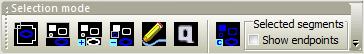
The icon buttons at the top determine how segments are selected or created. The first four buttons set the segment selection mode:
- Select chain selects all segments in a path. A path is defined as a sequence of segments where the start point of each segment is equal to the end point of the previous segment. For a closed path, you only need to select any part of the path. For an open path, you should select the beginning of the path. Previously selected segments will be deselected.
- Select selects all of the segments within the selection rectangle. Any previously selected segments will be deselected.
- Selection add selects all of the segments within the selection rectangle without deselecting any previously selected segments.
- Selection subtract deselects only the segments within the selection rectangle, leaving the remaining segments selected.
Use the left mouse button to draw a selection rectangle around the segments to select. Only segments on the Active layer (shown in blue) are selected. To change the active layer, choose a layer from the Active layer drop down list at the top of the Contour pane.
Note: Normally, only lines and arcs may be selected as contour objects. In order to select a round, oval, square, rectangle or rounded rectangle as a contour object, press the Ctrl key while selecting.
The next two buttons may be used to draw segments:
- Draw contour segment allows you to draw a contour segment manually. A straight line segment is created from the point where you press the left mouse button to the point where the mouse button is released.
- Quick contour allows you to draw a contour rectangle manually. Four straight line segments are created from the selection rectangle.
Drawn segments are used in the same manner as selected segments when creating a contour object.
Note: The two drawing modes may be useful if you have difficulties defining an outer contour, or if you simply want to do a quick import for the purpose of getting a price estimate.
The rightmost button clears all selected segments:
- Selection clear deselects all selected segments.
To delete contour objects, right click on the object and choose Delete or Delete all.
Drawing outline segments
Drawing outline segments BruceOutline segments may be drawn manually. This is especially useful if the active layer has an incomplete outline, where you need to close one or more gaps.
To draw an outline segment:
- Click on the Draw outline segment button.
- Move the mouse pointer to the position where the segment will start. If desired, press the X key to snap the mouse pointer to the nearest existing segment endpoint.
- Click and hold down the mouse button to start the drawn segment.
- Move the mouse pointer to the position where the segment will end. If desired, press the X key to snap the mouse pointer to the nearest existing segment endpoint.
- Release the mouse button to create the segment.
To draw a rectangle:
- Click on the Quick outline button.
- Move the mouse pointer to one corner of the rectangle. If desired, press the X key to snap the mouse pointer to the nearest existing segment endpoint.
- Click and hold down the mouse button to start the drawn rectangle.
- Move the mouse pointer to the opposite corner. If desired, press the X key to snap the mouse pointer to the nearest existing segment endpoint.
- Release the mouse button to create the rectangle.
Automatic outline definition
Automatic outline definition BruceIf a file has been linked to the Board outline layer, then an attempt will be made to automatically define the outer and inner (if any) contour objects. The auto-contour operation is performed after autolinking, or when switching to the Outline pane (if the outer contour is not yet defined).
Auto-contour does not work properly in all cases. Therefore, the outline should always be checked before publishing the imported product. In particular, automatically generated outline objects will have the default tool diameter specified with the Configure|Options menu command. If this is too large, then the objects must be deleted and re-created manually.
Auto-outline may be disabled by selecting the Configure|Automatic outline enabled menu item.
Board specifications
Board specifications BruceThe Specs pane is used to specify board properties, such as stackup, surface finish and silkscreen colors.
Click on the Select button to choose a stackup.
Choose a surface finish and colors for solder mask and legend. You can change the default values for these with the Configure|Options menu command.
If the board is to have hard (electrolytic) gold, specify the total area to have gold for each side.
Specify additional properties as appropriate.
If you have additional remarks that need to be passed on to the fabricator together with the production data, these can be entered either added to the Remarks layer or by using the File|Message to fabricator... menu command of the Import module.
If you are importing a board that is a revision of an existing product, you may use the Actions|Import board specs menu command and enter a product number. This will populate the board specifications and minimum feature sizes with values from the specified product.
Note: For single layer boards, it is not possible to link a soldermask file to the non-copper side of the board. In the Board Specifications pane, the soldermask color for the non-copper side will be set to None. Changing this to a color will indicate that the board should have soldermask on the non-copper side. This may increase the cost of the board.
Stackup selection
Stackup selection BruceThe Product layer buildup dialog box is used to choose from among the pre-defined layer builds, or to specify a custom build.
Click on a build number in the matrix to display an overview of the build. Right-click on the overview to view a detailed stackup drawing as a PDF file or to copy a simple diagram to the clipboard as text.
There are three types of builds:
- Free builds: These are builds where the total thickness and copper thicknesses are specified, but the distance between layers will be determined by the manufacturer. These builds are the least expensive.
- Constrained builds: These are builds where the thicknesses of all layers are specified.
- Custom builds: These are builds where each layer and material may be specified individually. A custom build may be specified as a free custom build or a constrained custom build. Note: For 0-2 layers, a custom build is always specified as a free build. Custom buildups are subject to approval by the manufacturer, who may suggest changes to improve manufacturability.
Specifying custom buildups in Macaos Enterprise
Specifying custom buildups in Macaos Enterprise Bruce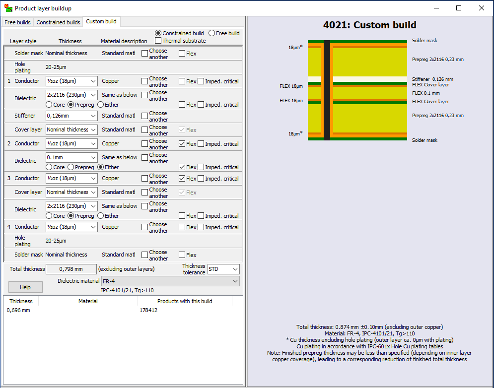
To specify a free custom build, specify the thicknesses for each conductor layer, and specify the total thickness.
To specify a constrained custom build, select or specify a thickness for each layer in the build.
Thicknesses may be selected from the drop down list or entered in the text box. An integer value will be interpreted as µm. A value with a decimal character will be interpreted as mm.
By default, custom builds are symmetric. When first specifying a thickness in the upper half of the build, the same thickness will be applied to the corresponding layer in the lower half of the build. In order for this function properly, all conductor and dielectric thicknesses should be specified before adding other layers to the build. Asymmetric buildups should be avoided, as this can lead to warping and other difficulties during manufacture.
The dielectric material for the build should be selected from the list at the bottom of the frame (to the right of the Help button). A wide variety of commonly used dielectric materials are included in the list. If you require a material that is not in the list, choose User defined (from the bottom of the list) and specify the material. The use of non-standard materials or thicknesses can greatly increase the cost and delivery time of the product.
The standard thickness tolerance is ±10%. Specifying a tighter tolerance will lead to higher costs.
At the bottom of the dialog box, there is a list of previously specified custom builds (if any). Select one of these to reuse the build in the new product.
Conductor layers
Select or specify a thickness for the conductor foil. The specified thickness should not include the thickness of hole plating. Plating is specified as a separate “layer.”
Conductor layers may be marked as flexible.
Conductor layers may be marked as having a thickness which is impedance critical.
By default, conductor layers are copper. To specify special requirements for the layer, check off for Choose another and enter the material name, manufacturer and/or description as desired.To edit the material description, right-click on the layer.
In the rare case where a multi-layer board has an odd number of copper layers, this must be specified by omitting one of the inner copper layers. For example, to specify a 3-layer board you should define a 4-layer build and specify Omit as the copper thickness for one of the inner layers.
Dielectric layers
Select or specify a thickness for the dielectric layer. The thickness of a dielectric layer may also be specified as a combination of prepreg sheets. Prepreg should be specified as follows:
qty x type [+ qty x type [+ qty x type]]
(without any spaces). For example, combinations such as 2x2116 or 1x1080+2x7628 are allowed. Valid prepreg types are 106, 1080, 2112, 2113, 2116, 2125, and 7628. Note: A nominal thickness is used for each prepreg type. The actual thickness may vary slightly depending on manufacturer.
Dielectric layers may be specified as core, prepreg or either. (If the thickness is specified as prepreg sheets, it will automatically be interpreted as prepreg when specified as either.)
Dielectric layers may be marked as flexible.
Dielectric layers may be marked as having a thickness which is impedance critical.
By default, dielectric layers use the material specified at the bottom of the frame (to the right of the Help button). To specify special requirements for the dielectric layer, check off for Choose another and select a material from the drop-down list.
Solder mask layers
Solder mask layers may only be added to the top and/or bottom of the build. Right-click on the desired conductor layer to add a solder mask. You need only add a solder mask layer to the build if you have special requirements.
The thickness may not be specified. Solder mask layers may be marked as flexible.
By default, solder mask layers use the manufacturer’s standard material. To specify special requirements for the layer, check off for Choose another and specify the material. To edit the material description, right-click on the layer.
Cover-layer layers
Cover-layer layers may only be added to conductor layers which are marked as flexible. Right-click on the desired conductor layer to add a cover-layer. You need only add a cover-layer layer to the build if you have special requirements, or for rigid-flex boards.
By default, the thickness is specified as Nominal thickness, which means that the manufacturer will use a suitable thickness. A different thickness may be selected or entered as desired. Cover-layer layers are always marked as flexible.
By default, cover-layer layers use the manufacturer’s standard material. To specify special requirements for the layer, check off for Choose another and specify the material. To edit the material description, right-click on the layer.
Stiffener layers
Stiffener layers may only be added to cover-layer or copper layers which are marked as flexible. Right-click on the desired layer to add a stiffener layer. You need only add a stiffener layer to the build if you have special requirements, or for rigid-flex boards.
By default, the stiffener thickness is calculated to give a total flex+stiffener thickness of 0.30 mm, if possible. A different thickness may be selected or entered as desired. Stiffener layers are not marked as flexible.
By default, stiffener layers use the manufacturer’s standard material. To specify special requirements for the layer, check off for Choose another and specify the material. To edit the material description, right-click on the layer.
Adhesive/bonding layers
Adhesive or bonding layers may be added above or below any layer. Right-click on the desired layer to add an adhesive or bonding layer. You need only add an adhesive or bonding layer to the build if you have special requirements.
By default, the layer thickness is specified as Nominal thickness, which means that the manufacturer will use a suitable thickness. A different thickness may be selected or entered as desired. Manufacturers usually know where and how to best make use of adhesive or bonding layers.
Adhesive or bonding layers may be marked as flexible.
By default, adhesive or bonding layers use the manufacturer’s standard material. To specify special requirements for the layer, check off for Choose another and specify the material. To edit the material description, right-click on the layer.
Plating layers
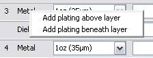 Plating layers represent the presence and thickness of hole plating in the buildup process. They are automatically added to the first and last conductor layer of builds with 2 or more layers. For sequential buildups or buried vias, plating should be added to the inner condcutor layers. To specify this, right-click on the layer and add plating above or beneath the layer (as appropriate). Missing or improperly placed plating layers will affect the display of buried vias in the product stackup drawing.
Note: When specifying plated inner layers, the inner layer (foil) thickness should be specified as 20 μm less than the desired layer thickness.
The plating thickness may not be specified. For IPC Class 1 or 2, plating shall be at least 20 μm thick. For IPC Class 3, plating shall be at least 25 μm thick. (For flexible layers, other rules apply.) Note that actual plating thickness can vary greatly from one place to another on the board, subject to plating process conditions. It is therefore not advisable to use a plated layer for impedance critical signal paths.
Metal-based boards
To specify a stackup for a metal-based board, check off for Thermal substrate (near the top of the frame). For a 2-layer build, you may choose a thermal Core rather than a thermal substrate at the bottom of the build.
Note: For metal-based boards, the material specified at the bottom of the frame (to the right of the Help button) specifies the thermal dielectric. It is not possible to specify special requirements for the dielectric layer(s) adjacent to the thermal substrate or thermal core.
Board statistics
Board statistics BruceThe Stats pane shows statistics for holes, routing, minimum features and other parameters. Parameters that can increase the cost of the product are highlighted with red text.
Minimum features
Minimum track width is the minimum width of electrical copper features on the layer. Minimum clearance is the minimum spacing between copper features on the layer. Minimum annular ring is the minimum ring width (pad radius minus hole radius) around plated holes on the layer.
Minimum track width and minimum annular ring are estimated by performing a simple analysis of the imported copper and drill layer data. Minimum clearance is estimated to be the same as the minimum track width. These estimates will be correct in most cases, but some CAD systems generate their trace and/or pad data in a manner that is too complex and timeconsuming for the rapid analysis performed by the Import module. Click on the hyperlink for more info about estimated minimum features.
If you know that one or more of the estimated values are incorrect, you should enter the correct values as necessary.
Note: If an estimated value is zero, then you must enter a value.
Note: If you have specified a stackup with a copper thickness larger than 1 ounce (35μm) then you may encounter restrictions on the allowed minimum track width or clearance. The minimum allowed track width or clearance on a layer is typically 2 to 3 times the copper thickness.
Note: Minimum feature sizes are used during price calculation, and if incorrectly specified may lead to incorrect price quotations. They are checked by the seller's CAM department prior to production, and actual prices will be adjusted if necessary.
Multi-board panels
If the product is a multi-board panel, specify the number of boards in the panel and the number of unique boards in the panel. Click on a hyperlink for more info about specifying board quantities.
Note: These values are used during price calculation, and if incorrectly specified may lead to incorrect price quotations. They are checked by the manufacturer's CAM department prior to production, and actual prices will be adjusted if necessary.
Board ID and Options
Board ID and Options BruceThe ID & Options pane is used to specify the product's name and description, and to specify product options as desired.
Product identification
A product must have a name. It may also have an article/stock/part number and/or a description.
If the manufacturer's packing system supports bar codes, the article number will be printed on the package labels both as text and as a bar code (unless the article number exceeds 20 characters). It should contain only English language letters, numbers, spaces, and the most common symbols (such as periods [.], hyphens [-] and slashes [/]).
Product options
Performance class: IPC, in the IPC-601x standards, has defined performance classes as a simple method of specifying tolerances and other quality requirements when manufacturing a PCB. The standard performance class is class 2, which is suitable for most applications. See here for more info.
Impedance control: If checked, then this product will require impedance control during manufacture. Impedance control is an added cost option.
Disallow manufacturer marking: If checked, then the manufacturer shall not add any identifying marks to the board. This option should not be selected if the board requires UL marks.
Copper shaving not allowed: If checked, then the manufacturer shall not retract copper from board edges or cutouts. Selecting this option implies that copper burrs along edges will be accepted. This option should only be checked in cases where it is necessary that copper extend to the board edges.
Padstacks
Padstacks BruceIn this mode you can view the shapes and sizes of all pads in a padstack. Click on a drill hole to view the padstack report.
Fiducial marks
Fiducial marks BruceIf a board is going to be sent through an automated (pick and place) assembly process, then the board should have at least one fiducial mark. A fiducial mark may be added by specifying the size and shape of the mark and clicking at the desired location. Press Ctrl+Alt when clicking to specify the location coordinates with the keyboard. Fiducials must not be placed too close to copper features or holes. If placed within a copper plane, an opening will be made in the copper. If a Pick&Place layer exists, the fiducial mark will also be indicated there.
Graphical remarks
Graphical remarks Bruce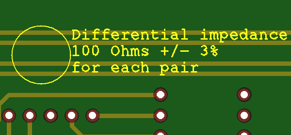
You may add remarks to a board. This is useful, for example, if there is some information about a specific region on the board which needs to be communicated to the manufacturer. To place a remark:
- Click on the Add remarks to board button to depress the button.
- Draw a circle around the area on the board to which the remark applies.
- Enter the text of the remark in the Place remark dialog box. Add line breaks as appropriate. The text will be placed to the right of the circle.
- Click OK to complete creation of the remark.
Use the Clear all remarks button to remove all remarks from the board.
Note: If you wish to add a remark which is not tied to a specific location on the board, you may use the Edit|Remarks to fabricator menu command.
Product number
Product number BruceThe manufacturer places a product/batch number at some position on the board, in order to identify the boards during production. If you wish, you may specify the position of this mark, rather than leaving it to the manufacturer to place the mark. The mark is normally placed on the legend top layer, but you may choose the bottom layer instead. If no legend layer exists, then the mark will be placed on a copper layer. If you choose not to place a mark, the mark will be placed by the manufacturer (unless there is not enough “empty” space on the board for the mark). To place a mark:
- Click on the Place Product/Batch number button to depress the button.
- Select the radio button for the desired layer.
- Select the Horizontal or Vertical radio button, or press Ctrl+R to change the text orientation.
- Place the rectangle at the desired location.
- Press Escape to exit the placement mode.
You should only place one mark on a board. For a panel of boards, a mark should be placed on each board in the panel.
Use the Clear symbols button or the Delete key to remove all marks.
Symbols
Symbols BruceA number of commonly used symbols may be added to the board. To add a symbol to the board, click on the Add symbols button and then do the following:
- Select the desired symbol.
- Select the radio button for the desired layer.
- Click and draw a rectangle for the bounding box of the symbol. (Doesn't apply to bar codes.)
- Right-click to cancel the operation, if desired.
- For a panel of boards, a symbol should be placed on each board.
Use the Clear symbols button or the Delete key to remove all of the current type of symbols.
The following symbols may be placed on soldermask or legend layers:
- UL mark. A bounding box is drawn where the manufacturer should place their UL mark. UL marks are specific to the factory, so only the boundary is displayed. By default, bounding boxes are restricted to one of several standard sizes. To create a smaller boundinig box, press Ctrl when clicking. Note: not all factories support smaller boxes.
- Lead-free symbol
- CE mark
- WEEE symbol
- Recycle symbol
- ESD-susceptibility symbol
- RoHS mark
- Annotation field. An annotation field is simply a solid rectangle, which may be used for laser etching or manual markings, such as serial numbers.
An annotation field may either be drawn as a rectangle or placed with a size suitable for a specific marking. To define the marking size, click on the Define button. This opens a dialog box for calculating the appropriate size for a text or bar code. You should enter a text similar (and with the same number of characters) as will be actually used.
Note: Two-dimensional bar codes use different encodings for a text with numbers-only, English alphanumeric text, or containing other-language characters. The actual bar code may differ in size from the sample displayed in the dialog if the sample text differs in number of character types.Note: For laser engraved 2-dimensional bar codes, we recommend a module size of 0.5 mm or larger.
Note: You should avoid placing an annotation field over copper traces if the annotation text will be laser engraved (due to the possibility of etching through the solder mask).
The following text formats may only be placed on legend layers:
- Bar code in Code 128-B format.
- 2D bar code in Data Matrix ECC 200 format.
Enter the bar code text in the edit box. The size of the bar code depends on the length of the text. Two floating rectangles display the size of the bar code and the surrounding quiet zone. Click to place the bar code. A bar code on the bottom layer is automatically mirrored.
The bar code will be in the soldermask color, with the legend color as the background color. For a dark legend on a light soldermask, this will result in an inverse image. Note: Many bar code reader apps do not support inverse images. We recommend the “ScanLife” app by Scanbuy, Inc., available at www.getscanlife.com. - A text string.
Enter the text in the edit box. A floating rectangle displays the size of the text. Click to place the text string. Text on the bottom layer is automatically mirrored.
A text string that complies with IPC/JEDEC standard J-STD-609A (for marking lead-free printed circuit boards) may be generated by clicking on the J-STD-609 button. This opens a dialog box where you may choose the material codes to include in the text string.
Note: Only ASCII characters from 32-127 are supported. This includes all digits, all letters in the English alphabet, and many symbols. Non-english characters or characters with accents or other diacritical marks are not supported.
Note: If the edit box is not visible, maximize the Import module window and/or use the Configure| Hide left sidebar and/or Configure|Hide right sidebar menu commands to increase the width of the graphic display.
Publishing a PCB product
Publishing a PCB product BruceOnce everything has been specified, the product may be published to the Macaos server. Prior to publishing, you must go through a checklist to confirm that all of the information is correct. You can use the check boxes to help you while going through the items. You must check off to confirm that you have reviewed items before the product may be published.
The checklist also lists the items that will be reviewed by the manufacturer once an order has been placed for the product.
Once the all items in the checklist have been checked and the checklist has been closed, a product number is assigned and the publishing process begins.
Normally, when a product is published, the user's company will be the owner of the product. If your company has partners, then you may choose one of your partners to be the product owner rather than your own company. See the Product sharing chapter for more information about partner management.
Once the product has been published and the product files have been uploaded to the server, the product product number is displayed and the product will be visible in the Never Ordered folder of the Product Browser, for pricing and order placement.
Stackup drawing
While generating the product files, a stackup drawing (in PDF format), including blind and buried vias (if any), will also be generated for the product.
If desired, you may specify your own text for the various fields of the drawing's title block.
Import options
Import options BruceChoose Configure|Options to modify the program configuration.
Default import folder and Default Export folder specify the starting folder for the File|Add files and File|Save to local disk commands.
The Default values settings determine the surface finish, solder mask color, legend color and outer/inner contour cutter diameter when importing a board.
Autolink state at startup specifies the autolink mode when the module is opened.
The Warn if estimated minimum features less than settings may be used to specify a value for minimum track/clearance and minimum annular ring. If the minimum feature estimator finds a value less than the specified minimum, then a warning message will be generated when publishing.
The Show help text option causes the help text panel to be shown when the module is opened.
The Run the File|New command option runs the File|New command when the module opens.
The Disable estimating minimum feature sizes option prevents estimation of minimum feature sizes. This may be useful if your CAD system generates larger objects by drawing them with many small, overlapping lines, thereby giving consistently incorrect estimates. When estimation is disabled, you must always enter the minimum feature size values before publishing.
The Show title block editor when creating stackup drawing option determines whether or not the editor will be displayed prior to creating a drawing. If you have previously selected Do not show this editor again, then this option allows you to re-enable the editor.